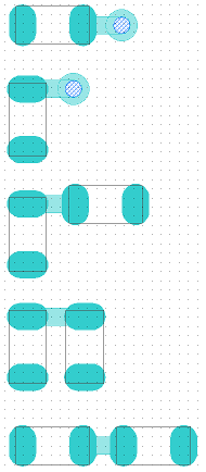
Chip Component Clearance Rules
This table shows safe minimum component clearances for reliable manufacture. This information is useful during circuit simulation when wanting to include lengths of microstrip line between components and vias.All distances are from PAD centre to PAD centre / VIA centre.
Via's are 0.63mm x 0.3mm.
 |
Component End to VIA |
|---|---|
| Component Side to VIA |
|
| Component Side to End |
|
| Component Side to Side |
|
| Component End to End |
