
Microstrip Clearance Guide
The data presented here reflects simulations done to aid in the layout of PCBs that use microstrip line.The simulation shows how the return loss of a length of microstrip line on FR4 is affected by the presence of ground walls either side of it. To mitigate the length of the line as a factor, the simulation is swept in frequency with a view to a worst case analysis.
Click the image for a larger view.
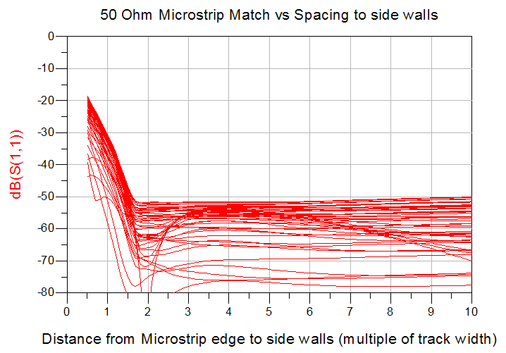
In general when laying out a PCB, a clearance of 1 track width to ground fill and vias is sufficient (30dB return loss from simulations).
Occasionally depending on the RF power involved and proximity of other sensitive circuits, 1.5 to 2 track widths should be used.
Allowing even greater clearance than this offers diminishing returns with length of line and frequency factoring strongly.